The use of PCB high pressure materials need attention:
Standards and precautions become stricter when creating PCBS for high-voltage dc bias. High voltage PCB materials and arc proof design ensure the safety and reliability of the final product. Avoid increased costs and risks by remembering these PCB materials and design tips.
High voltage PCB material:
The materials used in high-voltage PCB design need to maintain the best performance in the normal environment and over-voltage events as they age. Please consider the following materials for the main components of PCB:
PCB materials: when selecting materials for PCB, the PCB itself should be given priority. It provides the foundation for the rest of the PCB’s functionality, so weigh all the factors in the design before ordering the material. FR4 laminates provide very high dielectric breakdown, but they also have weak edge structures and are susceptible to contamination. BT epoxy provides good tolerability around, but because of its strong side walls, it is only suitable for specific applications. High pressure laminate has very high performance but also high price.
1) copper: the copper used to make PCB perforations shall have sufficient weight to withstand high current and mechanical stress. The PCB shall include heavy (4-10 oz) or extreme (10-50 oz) copper circuits and materials.
2). Resin and glass: although not technically the main PCB component, the level of resin and glass in the circuit board will affect its durability under high pressure. Circuit boards with high resin content and small glass style have the best dielectric performance.
To determine whether the material provides sufficient insulation to withstand high voltage dc bias, the comparative tracking index (CTI) was studied. The CTI of a material represents the voltage at which it begins to decompose in a standardized test. The companies that make PCB laminates do share the CTI data for their products in the data sheet. The CTI Numbers are divided into six categories, ranging from 0 (>, 600 V) to 5 (<100 V), with 5 indicating the lowest insulation level. Industry standards such as iec-60950-1 and ipc-2221 also mention recommended materials for high-voltage PCBS.
PCB high voltage material
Application of PCB high-pressure materials:
More industries than you might think need PCB that can withstand high pressure. Conditions such as low pressure cause the voltage to arc at an increased rate, so some applications that do not immediately use high current still require a well-designed PCB. The customer needs these PCBS for the following applications:
1). Spacecraft and other space equipment;
2). High-altitude aircraft;
3). High-tech laser;
4). Power supply of particle collider.
PCB high voltage material features:
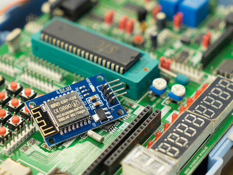
1).PCB high voltage material is mainly copper clad plate, and copper clad plate (copper clad plate) is composed of substrate, copper foil and adhesive. The substrate is an insulating layer composed of polymer synthetic resin and reinforced material. The surface of the substrate is covered with a layer of pure copper foil with high conductivity and good weldability, commonly used thickness of 35 ~ 50 / ma; The copper clad plate covered in one side of the substrate is called single-sided copper clad plate. The copper clad plate covered with copper foil on both sides of the substrate is called double-sided copper clad plate. Whether copper foil can be firmly coated on the substrate, by the adhesive to complete. Commonly used copper clad plate thickness has 1.0 mm, 1.5 mm and 2.0 mm three.
There are also more types of copper clad plates. According to the different insulation materials can be divided into paper substrate, glass substrate and synthetic fibreboard; According to the binder resin is divided into phenolic, epoxy, polyester and polytetrafluoroethylene, etc. It can be divided into general type and special type by use.
2).Copper-coated phenolic paper laminate:
It is a laminated product made of insulating impregnated paper (TFz 1 62) or cotton fiber impregnated paper (1TZ- 1 63) impregnated with phenolic resin by hot pressing. Mainly used as a printed circuit board in radio equipment.
3).copper-coated phenolic glass cloth laminate:
It is a laminated product made of alkaline glass cloth impregnated with epoxy phenolic resin by hot pressing. It is coated with copper foil on one side or both sides. It has the advantages of light weight, good electrical and mechanical properties and convenient processing. Its board face is flaxen, if use 3 cyanogen 2 make firm agent, then the board face is light green, have good diaphaneity. It is mainly used as printed circuit board in radio equipment with high operating temperature and operating frequency.
4).Copper-clad ptfe laminate:
Polytetrafluoroethylene plate as the substrate, the application of copper foil by hot pressure into a copper plate. It is mainly used as PCB in high frequency and uhf lines.
5).Copper foil epoxy glass cloth laminate:
It is the common material of hole metallized printed board.
6).Flexible polyester copper coated film:
It is a strip material made of polyester film and hot pressed with copper. In the application, it is curled into a spiral shape and placed inside the equipment. It is often poured as a whole with an epoxy resin for reinforcement or protection against moisture. Mainly used for flexible printed circuit and printed cable, can be used as a transition line connector.
PCB high pressure material design skills:
After selecting PCB materials, the manufacturer shall follow the design principles to increase its applicability to high-voltage dc bias:
1). Create a smooth surface finish to minimize the chance of arc;
2). Follow the safety standards of spacing;
3). Reduce the burr on the edge of the board after wiring;
4). Avoid sharp corners in trace lines and pad layout.
Clearance and creepage distance in PCB:
PCB in creepage distance and clearance in the measurement of the spacing requirements are very small. Arcs are easily formed between the two conductive elements of a PCB in a high voltage environment. Properly spaced components reduce the risk of arcing. The gap and creepage distance determine the spacing. A gap is the distance between two conductors through the air. If there is not enough clearance between the two conducting elements, an overvoltage event can create an arc between them. Creepage distance also indicates the distance between two conductors, but on the surface of the material rather than through the air. The correct creepage distance ensures that the components of the circuit board are not overcrowded.